
Бесплатно 
Sputnik Split Keyboard |Handwired Corne| ZMK |Ergo
MakerWorld

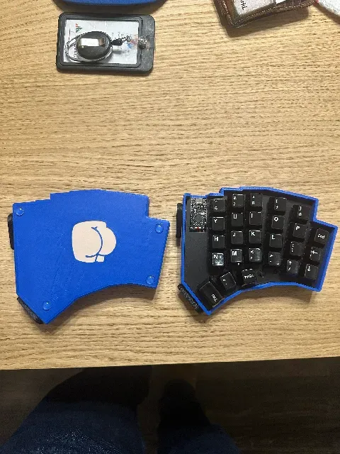
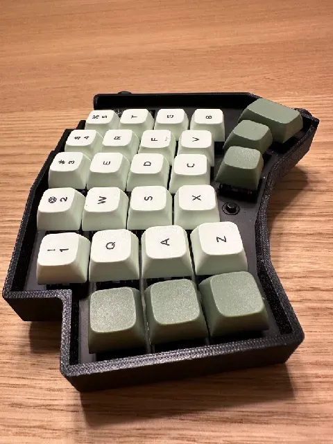


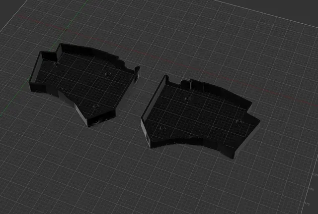


This repo is going to show the process of me designing, printing, working in KiCad, Fusion360, and overall building this split keyboard. I plan to explain the issues I didn’t know were issues until it was too late, and show how I managed to overcome some of the problems in the initial design.
Bill of Materials (Parts Used)
- 52x Akko Lavender Purple MX switches
- 52x Bojack 1N4148 diodes
- 2x nice!nano compatible microcontrollers (clones)
- 2x 250 mAh Li-Po batteries
- 2x latching power switch
- YMDK XDA profile keycap set
- M2 screws and Heat Set Inserts for assembly
- Socket headers for MCU
- Small gauge wire for BAT+ / BAT-
- Hand-designed Phanny PCBs (manufactured by PCBWay)
- 3D printed PLA+ case (plate & base)
The Design
KLE RAW Data
This board would not have come to life if not for Aran from PCBWay . He reached out to me to see if I had any interest in working on another project, this time utilizing their PCB manufacturing service. I enjoyed the work they did on a case I designed, and I love trying new things, so I took him up on his offer and got to work.
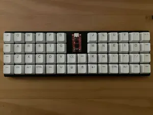
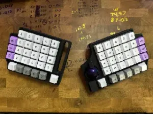
I knew the basics of what I wanted: split, ortho, staggered column, splay, and a num-row. I decided to get the layout dialed in using the well-known Keyboard Layout Editor I started playing around with different layouts and testing different splay angles. Then I adjusted how much column stagger I wanted. My aim was to make something comfortable when reaching for any key. Another issue I knew I wanted to overcome from prior boards was the thumb cluster. Thanks to printing several test plates, I think I landed on something very comfortable for long typing sessions while still leaving enough keys that I don’t feel forced into multiple layers.
KiCad
After finalizing my design, I moved into new territory: KiCad, a software program for designing circuit boards, schematics, and PCBs. I spent longer than expected trying to learn on the fly like I did with Fusion360, and that landed me with nothing but wasted time. I turned to YouTube and watched the tutorial videos from Modern Hobbyist Modern Hobbyist – Designing a Custom Keyboard PCB FROM SCRATCH and Joe Scotto How to Design Mechanical Keyboard PCBs with KiCad . Combined, their videos give enough of a breakdown that anyone could design a PCB, and both creators offer downloadable packages containing parts and footprints.
Schematic
The schematic editor was the easy part. It’s like designing a matrix—because it is designing the matrix—but instead of copper wire, it's pixels on a screen. This is where my lack of knowledge showed. I didn’t realize I could just copy the left, paste, then flip. So I ended up doubling my work.
Once I fixed all my errors, I clicked the PCB Editor and hit “Update PCB from Schematic.” Suddenly I had 52 MX footprints, 52 1N4148 diode footprints, and 2 nice!nano footprints neatly arranged. Thankfully, Modern Hobbyist’s video showed plug-ins that make placing switches based on Keyboard Layout Editor files much easier.
PCB Routing
Routing traces is basically a game of connect-the-dots, except the final picture is not a bear. This was challenging because you have to avoid blocking access to any other rows or columns. Pin by pin I worked through it until everything was connected and looking decent (to someone who knows nothing about circuitry).
Then came drawing the board outline. Adding “Edge Cuts” was another problem I discovered later. I rushed the design, eyeballed the right PCB instead of mirroring properly, and got bit in the ass designing the case.
Submitting to PCBWay
After fixing all visible errors, I sent the Gerber files to PCBWay using their plug-in. The system takes you to their site with the technical info pre-filled. You choose solder, solder mask color, silkscreen, and hit “Add to cart.”
Someone from PCBWay reviews your work and points out issues. My reviewer noticed I accidentally set huge mounting holes (2mm radius , not diameter) and fixed it. They also recommended thinning the break seam so both halves would snap cleanly apart. I happily let the experts help.
One week later, I had five pristine PCBs. Holding a board you designed—and having it look good—is a feeling I now crave. I went with flat black PCBs with white accents. Safe choice, great look.
Case Design
I exported my PCB from KiCad into Fusion360. I included all components so I could design around them with confidence (because I had already done enough guessing elsewhere).
A YouTuber I watch, Stuff Made Here, says something like: “Don’t design around a mistake instead of fixing it. It will cause more problems later.” I ignored that advice from someone who builds robots, the proceded to go through about twelve different case iterations until landing on the one I’m sharing here.
Assembly & Soldering
Time to solder and hope I correctly referenced the schematic.
Order of operations:
- Diodes (through-hole, top side)
- MCU socket headers
- Battery wires to BAT+ and BAT- Design flaw : I forgot a dedicated power connector
- Latching switch to battery and pads IMPORTANT : Positive to positive, negative to negative Best case: you fry an MCU Worst case: angry lithium fire rock
- Switches





Названия используются только для указания источника результата. Polyzon не аффилирован с перечисленными площадками.